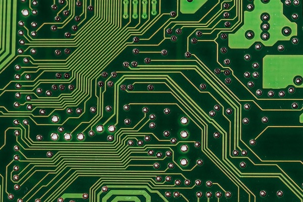
PCB circuit board etching processing method
As a 13-year etching processing factory, Hebei Weiyue has processed many PCB circuit boards. Today, I will introduce the methods of PCB circuit board etching processing. There are two types of PCB circuit board etching processing methods: one is etching of the inner layer; the other is etching of the outer layer.
The two types of PCB circuit board etching processing methods are mainly the difference between film negatives, one is a positive film, and the other is a negative film. Positive film used for inner layer etching and negative film used for outer layer etching.
The two PCB circuit board etching methods have different operating procedures:
When the first type of photosensitive ink is sprayed, the film is used to mask the areas that are not to be etched. During the exposure process, the parts that need to be etched are exposed, and then the substrate is cleaned by the developer and exposed to cure. The ink that is not etched will adhere to the substrate to protect it from corrosion. Etching is performed, and the ink is removed.
Another type of PCB etching process step is that the film protects the places that need to be etched, and the photosensitive ink on the places that don't need to be etched can resist corrosion after exposure. The ink on the place to be etched will fall off after being washed by the developing solution, and then the etching is performed.
Which two cases are suitable for two different PCB etching methods? Generally speaking, the products with inner layer etching generally have larger line width and line spacing, and the Ring ring is sufficient; while the outer layer etching is dense and the space is not enough. Within the purpose of making the line.
Chinese professional PCB circuit board etching processing manufacturer, welcome to contact Hebei Weiyue. We have imported foreign imported etching processing equipment and 6 automatic etching production lines to meet various batch and precision requirements. PCB circuit board etching processing has a wealth of etching for electronic products. Hands-on experience.
